6. Modeling at the RT level
Table of Contents
A register transfer level (RTL) design consists of a set of registers connected by combinational logic.

6.1. Combinational circuit
- A combinational circuit, by definition, is a circuit whose output, after the initial transient period, is a function of current input.
- It has no internal state and therefore is “memoryless” about the past event (or past inputs).
signal A, B, Cin, Cout : bit;
…
process (A, B, Cin) is
begin
    Cout <= (A and B) or ((A xor B) and Cin);
end;
6.1.1. To describe a combinational circuit
- The variables or signals in the process must not have initial values.
- A signal or a variable must be assigned a value before being referenced.
- The arithmetic operators (such as +, -, *, etc), relational operators (such as <, >, =, etc), and logic operators (such as and, or, not, etc) can be used in an expression.
6.1.2. Operator sharing
One way to reduce the overall size of synthesized hardware is to identify the resources that can be used by different operations. This is know as resource sharing.

sel <= c1 xor c2;

z <= a + b when sel=‘1’ else
    a + c;
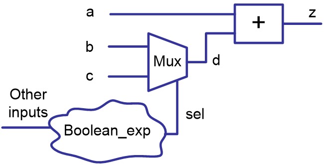
sel <= c1 xor c2;

d <= b when sel=`1` else c;
z <= a + d;
Performing resource sharing normally introduces some overhead and may penalize performance.
- In the above examples, assume T adder, T mux, T boolean
- For the circuit not sharing the adders: T = max ( T adder, T boolean) + T mux
- For the circuit sharing the adders: T = T adder + T :sub:`boolean + T mux
6.1.3. Shaping the circuit
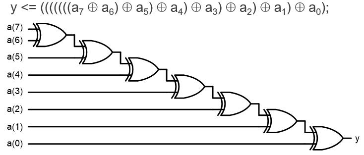
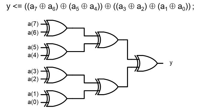
Using VHDL code, it is possible to outline the general shape of the circuit.
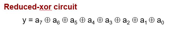
signal a: std_logic_vector (7 downto 0);
signal y: std_logic;
…
y <= a(7) xor a(6) xor a(5) xor a(4) xor a(3)
    xor a(2) xor a(1) xor a(0);
Examples
Combinational adder-based multiplier

The algorithm includes three tasks: * Multiply the digits of the multiplier (b4, b3, b2, b1 and b0) by the multiplicand A = (a4, a3, a2, a1, a0) one at a time to obtain b4*A, b3*A, b2*A, b1*A and b0*A.
bi * A = (a4*bi, a3*bi, a2*bi, a1*bi, a0*bi)
- Shift bi * A to left by i position.
- Add the shifted bi * A terms to obtain the final product.


More efficient description of an adder-based multiplier
6.2. Sequential circuit
- A sequential circuit is a circuit that has an internal state, or memory.
- Its output is a function of current input as well as the internal state. Thus the output is affected by current input values as well as past input values.
- A synchronous sequential circuit, in which all memory elements are controlled by a global synchronizing signal, greatly simplifies the design process and is the most important design methodology.
- Flip-flops and latches are two commonly used one-bit memory devices.
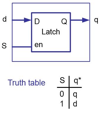
6.2.1. Latch
A latch is a level-sensitive memory device.
signal S, d, q: bit
……
process (S, d) is
begin
     if (S=‘1’) then
        q <= d;
     end if;
end process;
- In general, latches are synthesized from incompletely specified conditional expressions in a combinational description.
- Latch inferences occur normally with if statements or case statements.
- To avoid having a latch inferred, assign a value to the signal under all conditions.
signal S, d, q: bit
……
process (S, d) is
begin
     if (S=‘1’) then q <= d;
     else q <= ‘0’;
     end if;
end process;
asynchronous reset or preset An asynchronous reset (or preset) will change the output of a latch to 0 (or 1) immediately.
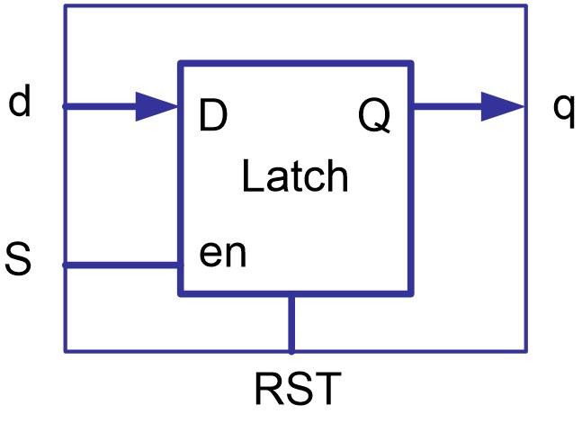
signal S, RST, d, q: bit
……
process (S, RST, d) is
begin
     if (RST = ‘1’) then
        q <= ‘0’;
     elsif (S=‘1’) then
        q <= d;
     end if;
end process;
6.2.2. Flip-Flops (f/f)
- A flip-flop is an edge-triggered memory device.
- To detect the rising edge (or falling edge), or the event occurred for a signal, we can make use of the attribute of a signal.
signal CLK : bit;
……
CLK’event                   true if CLK changes its value.
CLK’event and CLK = ‘1’     true for the CLK rising edge
CLK’event and CLK = ‘0’     true for the CLK falling edge
- The event attribute on a signal is the most commonly used edge-detecting mechanism. It operates on a signal and returns a Boolean value. The result is true if the signal shows a change in value.
Examples
a simple flip-flop
An edge triggered flip-flop will be generated from a VHDL description if a signal assignment is executed on the rising (or falling) edge of another signal.
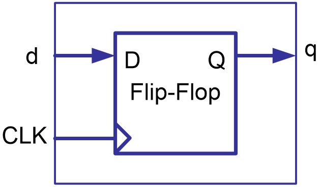
entity dff is
port (d, CLK: in bit; q: out bit);
end entity dff;
architecture behavior of dff is
begin
process (CLK) is
begin
     if (CLK’event and CLK=‘1’) then
        q <= d;
     end if;
end process;
end architecture behavior;
- Synchronous sets and resets
Synchronous inputs set (preset) or reset (clear) the output of flip-flops when they are asserted. The assignment will only take effect while the clock edge is active.

signal CLK, d, q, S_RST: bit;
……
process (CLK) is
begin
     if (CLK’event and CLK=‘1’) then
    if (S_RST = ‘1’) then
         q <= ‘0’;
    else
         q <= d;
    end if;
     end if;
end process;
- Asynchronous sets and resets
Asynchronous inputs set (preset) or reset (clear) the output of flip-flops whenever they are asserted independent of the clock.
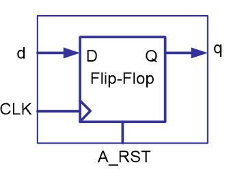
signal CLK , A_RST, d, q: bit;
……
process (CLK, A_RST) is
begin
     if (A_RST = ‘1’) then
        q <= ‘0’;
     elsif (CLK’event and CLK=‘1’) then
        q <= d;
     end if;
end process;
- A f/f with more than one asynchronous input

6.2.3. VHDL templates for sequential circuits
An RTL circuit can be described in two segments:
- A synchronous section updates the register information at the rising edge of the clock.
q_reg <= q_next; - A combinational section describes combinational logics, for example, update q_next;
- A synchronous section updates the register information at the rising edge of the clock.

Examples
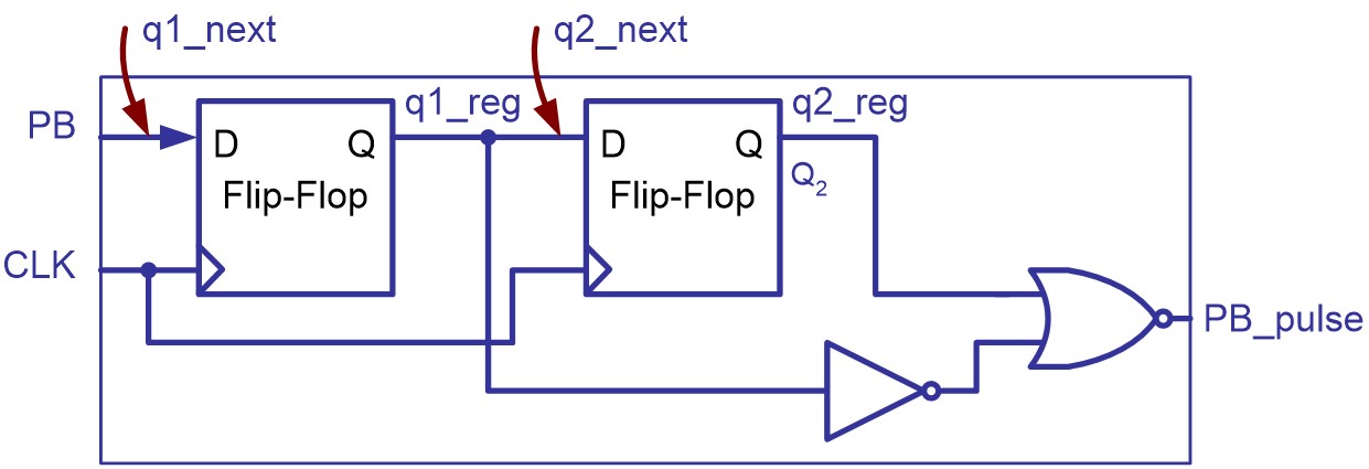
PULSER
6.2.4. Registers
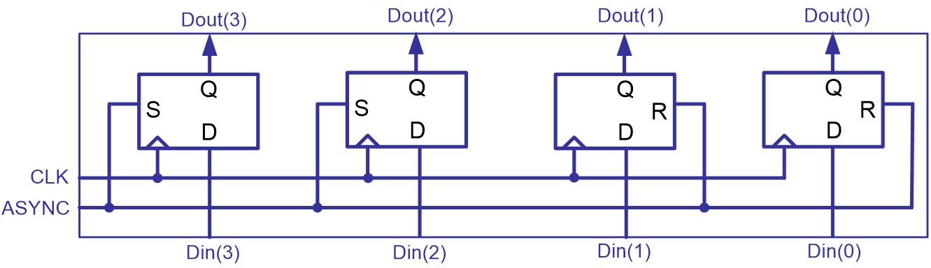
-- 4-bit simple register
signal CLK , ASYNC : bit;
singal Din, Dout :
    bit_vector (3 down to 0);
……
process (CLK, ASYNC) is
begin
     if (ASYNC = ‘1’) then
        Dout <= “1100”;
     elsif (CLK’event and CLK=‘1’) then
    Dout <= Din;
     end if;
end process;
Examples
4-bit serial-in and serial-out shift register
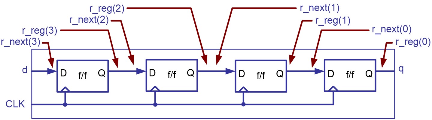
signal CLK ,d, q : bit;
……
architecture two_seg of shift_register is
signal r_reg, r_next: bit_vector (3 downto 0);
begin
process (CLK) is
begin
     if (CLK’event and CLK=‘1’) then
    r_reg <= r_next;
     end if;
end process;

r_next <= d & r_reg(3 downto 1);
q <= r_reg(0);
end architecture two_seg;
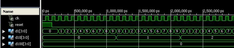
6.2.5. Synchronous counter
Examples
4-bit synchronous counter
Examples
Decimal counter
- A decimal counter circulates the patterns in binary-coded decimal (BCD) format.
- The BCD code use 4 bits to represent a decimal number.
Examples
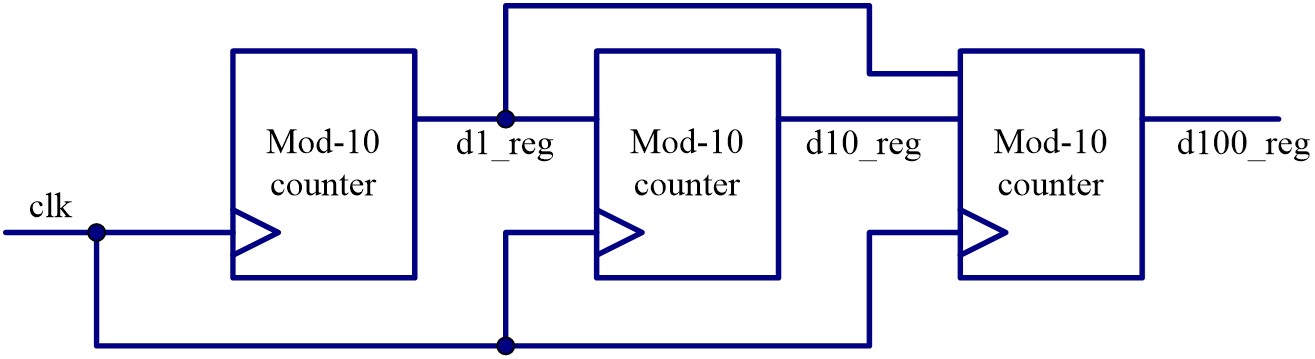
Three-digit decimal counter using conditional concurrent statements
Examples
Three-digit decimal counter using a nested if statement
6.3. Netlist of RTL components
A data path usually consists of a netlist of RTL components such as function units, multiplexers, comparators, registers, etc.

6.4. Test benches for sequential system
- All synchronous system require a system clock signal.
- A reset signal is required. The reset signal is asserted at power on to place the sequential system in its initial state.
6.4.1. Generating a system clock
Examples
50% duty cycle clock
clock_gen: process
    constant period : time := 100 ns;
    begin
            clk <= ‘0’;
            wait for period/2;
            clk <= ‘1’;
            wait for period/2;
    end process;
6.4.2. Generating the system reset
The reset signal typically
- starts in its asserted state at power on,
- remains in that state for a specified period of time, then
- changes to its unasserted state, and
- remains there for as long as power continues to be applied to the system.
The duration of the assertion of the reset signal is specified as
- either a fixed time
reset <= ‘1’, ‘0’ after 160 ns; - or some multiple of the clock’s period and is synchronized to the system clock
- either a fixed time
reset_process : process
begin
    reset <= ‘1’;
    for i in 1 to 2 loop
        wait until clk = ‘1’;
    end loop;
    reset <= ‘0’;
    wait;
end process;
6.4.3. Synchronizing stimulus generation and monitoring
use ieee.numeric_std.all;
signal x : std_logic_vector(3 downto 0); -- vector with element std_logic
signal y : unsigned(3 downto 0); -- vector with element std_logic
signal z : integer range 0 to 15;
--conversion between std_logic_vector, signed, unsigned
x <= y;  -- illegal assignment, type conflict
y <= x;  -- illegal assignment, type conflict
x <= std_logic_vector(y); -- legal assignment
y <= unsigned(x);  -- legal assignment
--conversion between signed, unsigned, integer
z <= to_integer(y); -- legal assignment
z <= to_integer(unsigned(x)); -- legal assignment
y <= to_unsigned(z, 4); -- legal assignment
x <= std_logic_vector(to_unsigned(z, 4)); -- legal assignment